SOLUTIONS
HFSS 3D Full Wave Simulation Capabilities
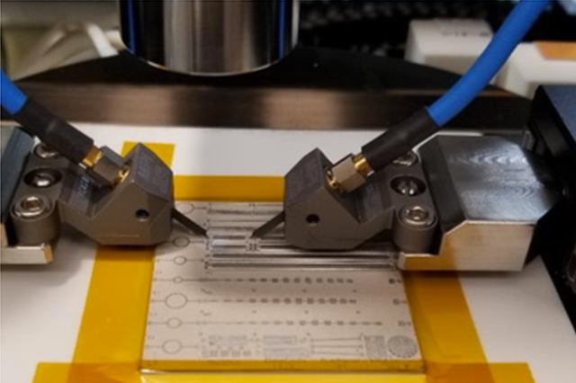
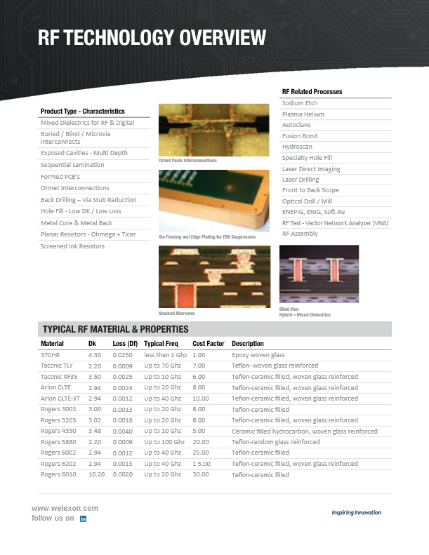
110 GHz VNA Test Capability
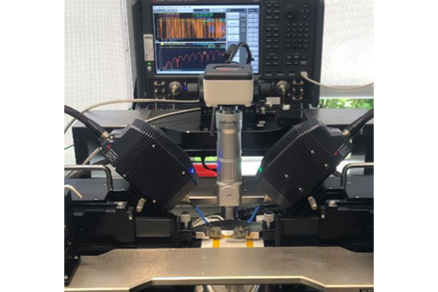
110 GHz VNA Test Capability
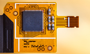
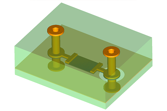
Multi-Functional Hole
Laser Drilling/Machining

All Xinger components have also been subjected to rigorous qualification testing
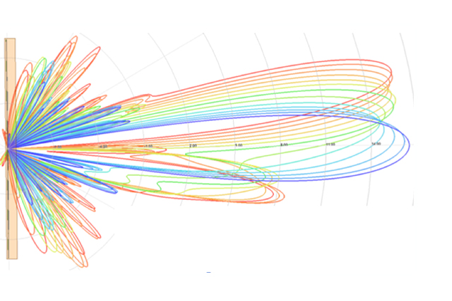
HFSS 3D Full Wave Simulation Capabilities
Buried Planar Resistor Technology
Buried Planar Resistor Technology

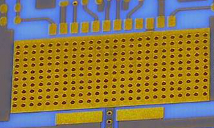
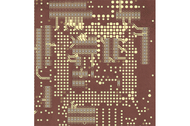
VIPPO Via-In-Pad-Plated Over
-
Our dedicated field applications engineers provide collaborative engineering support for the full product lifecycle, from inception to the field.
Qualifications/Certifications include; MIL-PRF-31032, AS 9100, ITAR, IPC 6012 & IPC6018, NADCAP, IATF 16949, ISO 9001, ISO 14001, ISO/IEC 17025, TL 9000-H, Bellcore Compliance, and OHSAS, as well as Automotive TS 16949 and Medical ISO 13485 certifications.
Contact Our Experts
Innovative brands trust WELEXON to bring their game-changing products to life. Are you looking for guidance on your next electronics application? Our experts are here to help.
NameCompanyEmailLocationYour Message